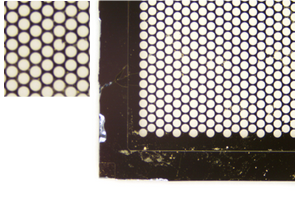
My position at the time involved making complex and delicate MEMS (microelectromechanical systems) components, with some elements about as thin as a healthy human hair. Of course, these are very delicate.
I noticed that there was an extreme yield loss that predated me, and surmised there was an issue in processing.

I worked with the technicians to catalog and understand the nature, frequency, and locations of the defects to establish a root cause.
It transpired that the majority of the issues was due to cracking in the outer region of each die, starting from the underside of the wafer.
This pointed to an issue with over-stressing the dicing interface. I increased the strength of the temporary adhesive used to mount the wafer to better support the delicate components, and adjusted the depth of cut to move the high-stress contact point deeper into the supporting handle material, to prevent the chipping that was ruining dies.
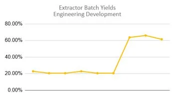
The results were plain - the yield jumped from 20 to 60% immediately. Over time, I made further refinements targeting other defects pushed the yield past 80%.